Lead the Semiconductor Revolution
Advanced Certification Programme in
Microelectronics and
Semiconductor Technology
Course offered by TalentSprint in collaboration with CCE at IISc

Course offered by TalentSprint in collaboration with CCE at IISc
"Tata Electronics and PSMC will build India's first state-of-the-art Fab unit in Dholera with a total investment of ₹91,000 Crores." 1

"Samsung launched a semiconductor R&D facility in India to drive cutting-edge semiconductor research and development in the country." 2

"With the approval of four projects, our combined production capacity will be 80 million chips per day, and with these, electronics manufacturing will jump from $105 billion to $300 billion in the coming years." 3
- Ministry of Electronics & Information Technology

"The demand for semiconductor jobs is on rise considering expansion plans of companies like Kaynes Technology, Micron Technology, and SRAM & MRAM Technologies contributing to12000+ new Jobs confirming the surge in opportunities." 4

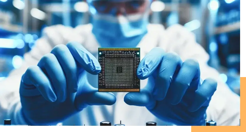
The Advanced Certification Programme in Microelectronics and Semiconductor Technologies offered by TalentSprint in collaboration with CCE at IISc. CCE at IISc offers courses suitably designed to meet the requirements of various target groups - research & development (R&D) laboratories and industries, research scientists, and engineers- enabling them to grow into competent managers of technology-intensive and data-driven organisations. http://cce.iisc.ac.in/
IISc (Indian Institute of Science) is the oldest and the finest higher education institute of its kind in India. It pursues excellence in research and education in several fields of Science and Engineering. It is one of the first three publicly funded institutes to be awarded the Institute of Eminence status. The alumni of IISc hold significant academic and industry positions around the globe. https://www.iisc.ac.in/


This comprehensive syllabus covering the latest industry practices and techniques on VLSI chip design is structured into two modules as a structured path spanning across the 2-month programme. Additionally, 1 week boot camp (hands-on practice) is planned after completion of the 2-month programme at IIT Hyderabad campus. This course curriculum is designed in a way that it aligns with the current industry trends and practices, making graduates job-ready and valuable to organisations. In addition, guiding the learners through the intricacies of the concepts with hands-on implementations on case studies and scenarios as per the industry standards. Each module (Digital/Analog) provides a solid foundation in building proficiency by ensuring a cohesive and thorough understanding from the basic to the advanced topics leveraging extensive hands-on implementations.
iPearl.ai (AI-Powered Interactive Platform for Experiential And Remote Learning), TalentSprint Digital Delivery has been architected to incorporate best-of-breed technologies and state-of-the-art components.
The hallmark of the platform is its seamless integration of diverse but related learning technologies that facilitates synchronous learning, asynchronous learning, assignments, assessments, group work, cloud labs, and video indexing, with just one single sign-on. This maximizes user delight, for both students and instructors.
Learn from India's leading semiconductor researchers

Professor, Department of Electronic Systems Engineering, IISc
Co-Founder – AGNIT Semiconductors Pvt. Ltd and Gallium Nitride Ecosystem Enabling Center (GaN Fab)
Hear directly from learners who joined to advance their careers in semiconductor technology.
"I am interested in Microelectronics and Semiconductor Technologies for its focus on high-performance microchips used in daily devices. The esteemed course by CCE at IISc will equip me with the necessary skills to contribute to this growing field."
"I have 8+ years of experience in SOC validation and am eager to expand my knowledge in semiconductors. This comprehensive program will help me gain more expertise and improve my technical skills/capabilities, allowing me to meet industry demands and advance in my career."
"I have 15+ years of experience as an Electrical & Instrumentation Specialist. I now seek academic depth and sophistication, which the Advanced Certification Program in Microelectronics and Semiconductor Technologies at CCE-IISc can provide in the field of semiconductors."
Note: These are edited versions based on the details submitted by various programme applicants.
Minimum Qualification: B.E./B.Tech Degree (ECE, EEE, EE, Instrumentation, Nanoscience, Material Science, Material Engineering or M.Sc. in Electronics/Physics).

Our programme offers two distinct tracks, each tailored to meet different learning goals and career aspirations.
Advanced Certification
Programme in Microelectronics &
Semiconductor Technologies
Executive Certification
Programme in Microelectronics &
Semiconductor Technologies

Master the art of designing and fabricating cutting-edge semiconductor devices.

Build products that integrate machines, workers, energy, material and data.
Build and foster a team capable of designing nano-scale semiconductor devices.
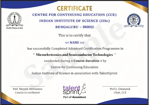
Supports program alumni looking for new career advancements.



Advanced Certification
Programme in Microelectronics and
Semiconductor Technologies
Starting at ₹14,828 / Month
Executive Certification
Programme in Microelectronics and
Semiconductor Technologies
Starting at ₹10,591 / Month
(i) *Fees paid are non-refundable and non-transferable.
(ii) *18% GST extra as applicable.

TalentSprint, Part of Accenture, is a global leader in building deep expertise across emerging technologies, leadership and management. Through innovative learning programs and strategic partnerships with premier academic institutions, TalentSprint empowers professionals to accelerate their careers.
With over 15 years of excellence, TalentSprint has helped thousands of learners transform their careers through industry-focused programs in AI, Semiconductor, Cybersecurity, Data Science and other next-generation technologies.

National AI Olympiad
AI Infinity
India Smart University Awards
India Smart University Awards
India Smart University Awards
India Smart University Awards
India Smart University Awards

India Smart University Awards

India Smart University Awards

India Smart University Awards

India Smart University Awards
India Smart University Awards
India Smart University Awards
India Smart University Awards

India Smart University Awards

India Smart University Awards

India Smart University Awards

India Smart University Awards
Microelectronics and Semiconductor Technologies are enabling the creation of next-generation semiconductors, making systems faster, smaller and more energy efficient.
The majority of professionals in the VLSI and semiconductor industry are often trained in VLSI design or circuit design principles, and in their design practice, they consider semiconductor devices as a black box. These design practices, which require one to follow thousands of design rules, don’t involve a first principal understanding of semiconductor technology. This gap originates from the undergraduate and postgraduate training given at the majority of places, which lacks rigorous training on micro and nanoelectronics and device as well as semiconductor technology principles. While the black box approach may have worked for several generations, given the way technology is advancing, it is going to be difficult for working professionals to survive in this industry without understanding the fundamentals of devices and semiconductor technologies and the principles of micro and nanoelectronics. The other aspect is the push for semiconductor fabs and production around the world. There will be around fifty new fabs in the next 5 years, possibly even more, and each fab would require thousands of semiconductor professionals. This means there will be demand for over one lakh new professionals in the next five years who understand semiconductor technologies. To enable professionals to navigate this change, The Semiconductor Industry is expected to reach $958.93 billion by 2030 ~ Mordor Intelligence, where aspirants can enhance their knowledge and build capabilities to thrive in the new semiconductor era.
A tech professional in semiconductor/VLSI domain, or across any electronics industry, keen to build expertise in design, development, and integration of micro and nanoelectronics devices and semiconductor technologies. An industry professional or Engineering Manager willing to build a leadership career in the semiconductor industry. An academician who wants to build practical expertise in semiconductor technology and enrich their academic and research portfolio. A fresh graduate willing to build a career in Microelectronics and semiconductor industry.
With the growing complexity of CMOS technology and the increasing importance of heterogeneous integration, a strong grasp of semiconductor technology has become essential for appreciating the intricacies of circuit design and its performance dependencies on technology- and device-specific knowledge. A thorough understanding of semiconductor technology not only enhances efficiency in circuit design for advanced nodes and complex or heterogeneously integrated automotive nodes but also deepens insight into process, technology, and device design principles. This comprehensive knowledge is crucial for navigating complex circuit design rules. In essence, mastering semiconductor technology significantly elevates your capabilities as a circuit designer and opens opportunities to lead at the semiconductor/technology forefront.
For every module there will be an MCQ based test and also at the end you would be working on a project suggested by the professor.
The programme duration is 9 months and includes live online classes, self-paced learning, assignments, projects and hands-on laboratory sessions.
Most learning is delivered online through live interactive sessions. Certain laboratory activities or campus visits may be scheduled depending on the programme structure.
Sessions are delivered by IISc faculty, experienced researchers, industry experts and semiconductor professionals with extensive real-world expertise.
Candidate submit their application forms for the program by sharing details of education, work experience, and a statement of purpose. These applications are reviewed by IISc faculty members corresponding to their respective programs. A selected candidates list issued by the IISc faculty members and the candidates are informed by the TalentSprint team through a selection email. A payment link for paying the program fee is shared along with the selection email. Candidates can enrol into the program by making payment of the program fee.
Join in these easy steps: Minimum Qualification: B.E./B.Tech Degree (ECE, EEE, EE, Instrumentation, Nanoscience/Nanotechnology, Material Science, Material Physics, Material Engineering and Semiconductor) Marks: Minimum of 50% marks and good exposure to physics Experience: Minimum of 2 years
As per the programme norms, participants have to maintain at least 75% of attendance during the programme. Going by the curriculum, it is recommended that participants maintain attendance for enriched learning. In the event of unavoidable circumstances, if any, one can access the recorded lectures on our platform to cover up for the missed sessions.
Yes. Flexible EMI options can be availed to pay the programme fee in installments. Please reach out to your RM to know about the details of the schemes available.
No, the application fee is non-refundable.
The tried and tested direct-to-device platform enables 24 x 7 learning for its users. Some key benefits of the platform are: Intuitive student experience through a user-friendly LMS Seamless faculty experience through state-of-the-art Studios Highly Interactive Online Classes Effective group/peer learning/projects through Breakout Rooms Proctored Online Assessments with detailed analysis Insightful Reports on student engagement and performance Flexible integration with other components, as needed
An internet-connected device, Computer/Laptop/Tablet/Smartphone, is enough to access the platform and Web camera and Mic with necessary power backup will be needed for proctored online assessments.